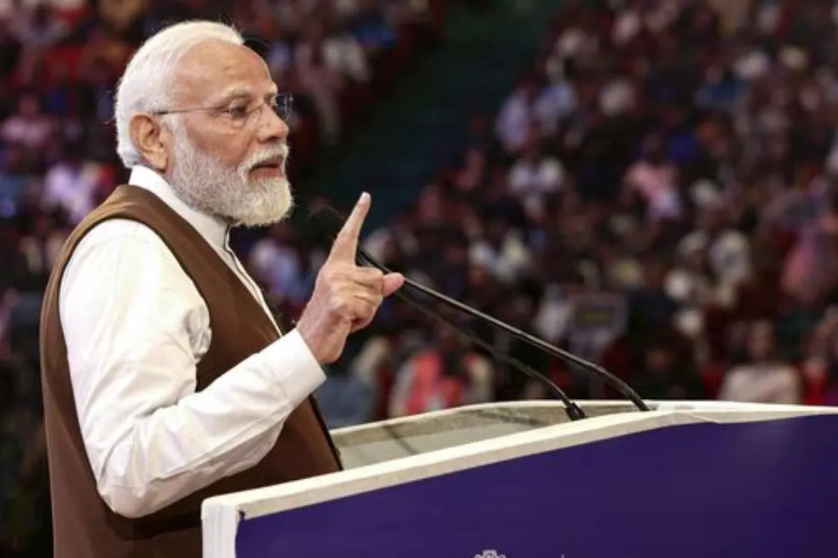
PM Modi: Union Minister of Education Dharmendra Pradhan said on Twitter that Prime Minister Narendra Modi will be laying the foundation stone for three semiconductor facilities tomorrow, March 13. With an estimated cost of ₹1.25 lakh crore, these cutting-edge facilities represent a major step towards making India a global leader in electronics design, manufacture, and technology.
Strategic Significance of Semiconductor Facilities
The tweet draws attention to the event’s twin objectives. In order to strengthen India’s standing in the international electronics industry, it first highlights the strategic significance of these semiconductor facilities. By making investments in state-of-the-art semiconductor technology, the nation hopes to become competitive and independent in the quickly changing tech sector.
Second, there is a plan to address kids in conjunction with the ceremony to lay the foundation stone. Along with opening these state-of-the-art facilities, Prime Minister Modi will interact with the youth. By connecting the government’s programmes with the goals of the nation’s vibrant youth, this engagement seeks to inspire and guide the youth.
Revolutionizing the Electronics Industry
It’s expected that the construction of these semiconductor facilities will revolutionise India’s electronics industry by stimulating innovation, R&D, and creativity. It is also anticipated to create a significant number of job opportunities, supporting the government’s goal of a technologically advanced and independent Bharat.
In his tweet, Dharmendra Pradhan exhorts the gifted #YuvaShakti, particularly college students, to get involved in this important initiative. The goals of a developed India and technical advancement are reflected in the hashtags #Techade and #ViksitBharat.


